top of page

Temporary Bonding

The demand for higher functioning chips at smaller dimensions and operating cool is one of the top challenges in meeting growth by AI, data centers, and EVs.  Companies are driving their substrates to be thinner and supported by carriers.  This isn't new, yet the dicing of multi-layered thin chips present issues as they become thinner. Imagine saw-cutting a piece of paper, lasering through a multi-stack comprising metal and organic without thin film voiding, and finally, conformal protection of bumped wafers having feature variations nearly 50um. These and more are challenges supported by Daetec. 


Flexible Displays
Thin substrates that peel
Transparent Films
Packaging heterogenous devices for higher functionality
Solar Cells
Solar substrates that are thin, flexible, and transparent
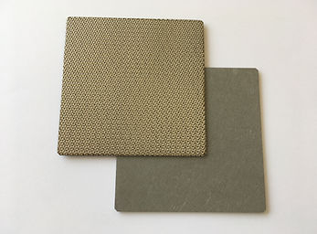
Porous Carriers
Porous or Rinseable Carriers
Anchor 1

Cleaning

Daetec is an expert consultant in the fields of cleaning and rinsing. We support moving away from chemical intensive processes; instead, we shift our customers to water rinsing that's faster and cleaner. Daetec uses our subcontracted factories for support, located in the USA and Asia.

Dry Film PR Stripping
Rinsing of dry-film photoresist
Aviation Polysulfide Removal
Polysulfide sealant removal used in fuel tanks
Thick PR Stripping
Photoresist rinsing
Eco-Friendly Products
Environmentally safe and low cost rinsing
Anchor 2
Contact us

Daetec, LLC

799 Main St., Unit F

Half Moon Bay, CA 94019

USA

​​

Tel: (805) 630-0779

​​​

email: jmoore@daetec.com

Have a question? 

Don't hesitate to contact us! 

  • Facebook Social Icon
  • Twitter Social Icon
  • Google+ Social Icon
  • YouTube Social  Icon
  • Pinterest Social Icon
  • Instagram Social Icon
bottom of page